Thermal Management for 400G, 800G & 1.6T Optical Transceivers: Critical Challenges and Advanced Cooling Solutions
An optical module is typically composed of optical transmitting components, optical receiving components, functional circuits, and optical (and electrical) interfaces. At the transmitting end, a driver chip processes the raw electrical signal and drives a semiconductor laser (LD) or Light Emitting Diode (LED) to emit a modulated optical signal.
What is the Structure of an Optical Transceiver?
Overview of Composition:
An optical transceiver (commonly referred to as an optical module) is primarily constructed from an optical transmitting device, an optical receiving device, functional circuitry, and optical/electrical interfaces.
On the transmission side: A driver chip processes the raw electrical signal and drives a semiconductor laser (LD) or Light Emitting Diode (LED) to emit a modulated optical signal.
On the reception side: Upon entering the module, the optical signal is converted back into an electrical signal by a photodiode. This signal is then processed through a pre-amplifier before being output as a usable electrical signal.
Detailed Component Breakdown:
1. TOSA (Transmitter Optical Sub-Assembly):
The core component here is the Laser Diode (LD), responsible for converting electrical signals into optical signals. Common laser types include FP, DFB, EML, and VCSEL.
2. ROSA (Receiver Optical Sub-Assembly):
The core component is the Photodetector (PD), tasked with converting received optical signals back into electrical signals. Common detector types include PIN and APD.
3. PCBA (Printed Circuit Board Assembly):
This serves as the brain of the module, housing the driver circuits, signal processing units, and power management systems. Crucially, it supports DDM (Digital Diagnostic Monitoring) functionality for real-time health checks.
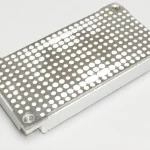
4. Enclosure (Housing):
Typically made of metal, the enclosure serves three critical functions: securing internal components, shielding against Electromagnetic Interference (EMI), and facilitating effective heat dissipation to ensure thermal stability.
5. Optical Interface (Receptacle):
The physical port used to connect optical fiber patch cords (common interface standards include LC, SC, and MPO).
Key Performance Indicators (KPIs) of Optical Transceivers
1. Analysis of Key Transmitter (Tx) Indicators
Average Output Power :
Refers to the average optical intensity emitted during normal operation.Impact: If power is too low, the signal won’t reach far; if too high, it might “blind” the receiver or accelerate laser aging.
Note: It must be balanced with receiver sensitivity to ensure successful transmission.
Extinction Ratio (ER):
Measures the laser’s ability to distinguish between a “1” (light on) and a “0” (light off).Impact: Low ER means the distinction is blurry, causing the receiver to misinterpret signals (Bit Errors). However, an excessively high ER can introduce other signal integrity issues (like chirp). A balanced range (typically 8.2dB to 10dB) is ideal.
Center Wavelength:
Just like a radio station frequency, optical signals have specific wavelengths (e.g., 850nm, 1310nm, 1550nm).Critical: You must ensure the wavelength matches the fiber type (Single-mode vs. Multi-mode) and the receiver at the other end. Mismatches lead to communication failure.
2. Analysis of Key Receiver (Rx) Indicators
Receiver Sensitivity :
The minimum optical power the receiver can detect while maintaining a specific Bit Error Rate (BER).The Math: Usually expressed in negative dBm (e.g., -22dBm). A smaller number (larger absolute value) means the receiver is more sensitive and can “hear” fainter signals from further away.
Overload Optical Power (Saturation Point):
The maximum input power the receiver can handle.Analogy: If the incoming light is stronger than this limit, the receiver becomes “saturated” (blinded), causing errors. It’s like being deafened by a loud explosion.
Input Optical Power Range :
For a stable link, the incoming signal power must fall safely between the Sensitivity (floor) and the Overload Point (ceiling).
3. System-Level & Physical Reliability Indicators
Data Rate & Distance:
Rate: Must match your switch port (e.g., 1.25G, 10G, 100G).
Distance: Limited by Attenuation (energy loss) and Dispersion (signal spreading). You must select the right module spec based on your actual cabling distance.
Physical Compatibility ):
Ensures the module fits your hardware. Key factors include Fiber Type (Single-mode for long-haul, Multi-mode for short-reach) and Interface Type (LC, SC, MPO).Reliability Metrics :
Power Consumption: Directly relates to Heat Dissipation. Higher power requires better thermal management designs.
Operating Temperature: Commercial (0
70°C) vs. Industrial (-4085°C) grades.Lifespan: The industry standard for MTBF (Mean Time Between Failures) is typically 50,000 hours (approx. 5 years) of 24/7 continuous operation.
Summary of Optical Transceiver Performance Indicators
| Performance Category | Key Metrics / Core Indicators | Core Function & Significance |
| Transmitter (Tx) Performance | Average Output Power, Extinction Ratio (ER), Center Wavelength | Ensures that electrical signals are efficiently and accurately converted into high-quality optical signals for transmission. |
| Receiver (Rx) Performance | Receiver Sensitivity, Overload Optical Power (Saturation Power), Input Optical Power | Ensures accurate detection of optical signals across a dynamic range (from weak to strong) and restores them into clear electrical signals. |
| Overall Link Performance | Data Rate, Transmission Distance (Reach) | Determines the module’s data transmission capacity and coverage range; serves as the fundamental basis for model selection. |
| Physical & Reliability | Fiber Type, Interface Type, Operating Temperature, Power Consumption, Lifespan (MTBF) | Ensures compatibility with your hardware infrastructure and guarantees stable operation throughout the expected lifespan. |
The Impact of Temperature Extremes on Optical Transceivers
Temperature is a critical KPI for optical transceivers, significantly affecting both performance and lifespan. The impact is primarily divided into two scenarios: Overheating (High Temperature) and Freezing (Low Temperature).
1. Issues Caused by Excessive Heat
High temperature is the primary enemy of electronics. Here are the common consequences:
Accelerated Device Aging :
High heat accelerates the aging process of internal components. It increases power consumption, which in turn generates more heat, creating a “Thermal Runaway” scenario. This ultimately leads to overheating and catastrophic burnout.Performance Instability & Data Errors:
Under high heat, the module’s nominal performance may drift, leading to operational instability. This results in Bit Errors or packet loss, increases the failure rate, and significantly shortens the MTBF (Mean Time Between Failures).Optical Power Anomalies:
Heat can cause Tx power to drift high or low, while Rx Sensitivity degrades. This leads to increased Noise and Signal Distortion. In extreme cases, the laser or detector can be permanently damaged.Defocusing and Misalignment :
Expert Note: Due to the Coefficient of Thermal Expansion (CTE) mismatch, internal components expand at different rates. This causes the precise optical path to shift or defocus, preventing the TOSA/ROSA from achieving expected coupling efficiency.APC Failure :
Elevated temperatures can cause the APC (Automatic Power Control) circuit to lose regulation. The Bias Current may spike drastically to compensate for laser efficiency drop. Once it exceeds the monitoring threshold, the module may lock up or burn out the Driver IC or the Laser Diode.
2. Issues Caused by Low Temperature
While less common, extreme cold also poses risks:
Degradation of Optical Performance :
Low temperatures alter the electrical and mechanical properties of materials. This can lead to reduced Tx power, worsened Rx sensitivity, and increased signal distortion.Contraction-Induced Misalignment :
Materials contract in the cold. For high-precision modules (like Single-mode), even microscopic shrinkage can cause significant Optical Misalignment (focus shift), severely impacting signal quality.Material Embrittlement :
Certain adhesives and packaging materials may become brittle at freezing temperatures, leading to Micro-cracks or structural fractures that compromise the hermetic seal and integrity of the module.
3. Root Causes of Temperature Anomalies
Ambient Temperature :
The external environment is a major factor. High room temperature, outdoor heat, or proximity to other heat sources (like CPU heatsinks) will raise the module’s baseline temp. Conversely, improper cooling in extreme cold affects start-up performance.Thermal Design Efficiency :
Expert Note: This is critical. Poor thermal design—such as an undersized Heatsink, inefficient Airflow path, or poor Thermal Interface Material (TIM) application—leads to heat accumulation.Circuit Design & Power:
Excessive current draw or low resistance traces leads to Joule Heating. Conversely, open circuits or under-current can cause abnormal cold operation (non-functioning).Operational Load:
A module under full traffic load (100% duty cycle) generates significantly more heat than one in idle or low-traffic states.
Optical Transceiver Thermal Management Solutions
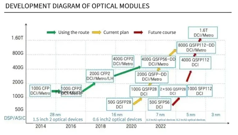
As optical transceiver speeds migrate from 100G to 400G and 800G, power consumption has skyrocketed—high-end modules now frequently exceed 20W. If this heat is not effectively dissipated, it leads to signal degradation and drastically shortens the module’s lifespan (MTBF).
Effective thermal management faces 4 Core Challenges
1. Suffocatingly Constrained Space (High Volumetric Density)
The Constraint: Optical transceivers must adhere to strict industry Form Factors (e.g., SFP+, QSFP28, QSFP-DD, OSFP).
The Reality: Taking the common QSFP28 as an example, its dimensions are merely 18.3mm × 56.5mm × 13.6mm—roughly the size of half a cigarette lighter.
The Problem: There is virtually zero room to accommodate large heatsinks or active cooling mechanisms inside the module.
2. Concentrated Heat Sources & “Thermal Islands”
The Culprits: The primary heat generators—Laser Diodes (LD), Driver ICs, and the DSP (Digital Signal Processor)—are all crammed onto a tiny area of the PCB.
The Physics: This creates extreme High Heat Flux, where localized temperatures can soar 30-50°C above the ambient temperature, forming isolated “High-Temperature Islands” that are difficult to cool uniformly.
3. Extreme Ambient Temperature Fluctuations (” The Rollercoaster”)
The Requirement: Industrial-grade modules must operate flawlessly between -40°C and +85°C.
The Dilemma:
At High Temps: Dissipation efficiency drops, risking overheating.
At Low Temps: The system must actually generate heat (via internal heaters or TEC) to maintain laser stability.
The Challenge: Managing this dual requirement of “Cooling vs. Heating Compensation” doubles the complexity of the thermal design.
4. The Interface Bottleneck (“The Narrow Bridge”)
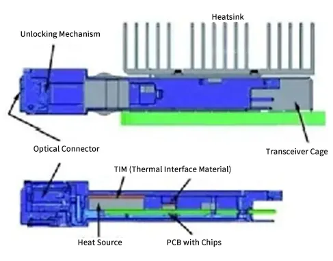
The Path: Heat must primarily exit through the Gold Fingers (Electrical Interface) and the contact points with the switch’s Cage.
The Bottleneck: These contact areas are small and often have high Contact Thermal Resistance. Trying to channel 20W+ of heat through these limited pathways is like forcing a flood through a narrow bridge—efficiency is significantly compromised.
5 Core Technologies – Solving Heat from "Source" to "Exhaust"
1. Optimization of Thermal Conduction
The “First Mile” of Heat Transfer:
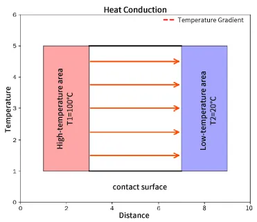
The initial journey of heat from the Chip (Source) to the Heat Carrier must be an unimpeded “highway.” The core objective here is to Minimize Contact Thermal Resistance:
| TIM Type | Thermal Conductivity ( | Ideal Applications | Key Benefits |
| Thermal Silicone Pad | 1 – 10 | Fixed Gap Scenarios<br>(e.g., General PCB components to case) | • Electrical Insulation• Easy Assembly • Reworkable |
| Thermal Gel | 5 – 30 | Irregular Gaps & Automated Lines(e.g., Chips with varying height tolerances) | • High Conformability • Low Thermal Resistance • Low Stress on components |
| Metal Thermal Pad (Indium) | 80 – 100 | High-Power Modules (e.g., 800G)(High heat flux applications) | • Superior Conductivity<br>• High Ductility |
Chip Direct-to-Metal (D2M) Mounting
Bypassing the PCB Bottleneck:
Unlike the traditional method where the chip is mounted on the PCB first (forcing heat to travel through the board), D2M technology mounts the chip directly onto the metal enclosure or heatsink.
The Result: This bypass strategy shortens the Thermal Path by 30-50%.
Best For: It is the ideal solution for High-Heat Flux components (the “high fever” parts) such as DSPs and Laser Diodes (LDs), drastically lowering the Junction-to-Case thermal resistance(
Rjc).
2. Optimization of Thermal Spreading
Spreading the Heat: Eliminating Lethal Hotspots
Localized high temperatures (Hotspots) are fatal to optical performance. The goal is to distribute this concentrated heat across a larger surface area via the PCB and metal structures.
Optimization of PCB Structure
Heavy Copper Technology:
Upgrade the copper weight in critical zones from standard 1oz (35um) to 2-4oz (70-140um).The Physics: Copper has a thermal conductivity of 401 W/(m·K), which is over 200 times higher than the FR4 PCB substrate. Thicker copper acts as a super-highway for lateral heat spreading.
Embedded Copper Coins / Micro Heat Pipes:
Embed micro heat pipes (e.g., 2mm diameter) directly inside the PCB layers.Expert Insight: With an effective conductivity exceeding 10,000 W/(m·K), heat pipes function as “superconductors,” rapidly transporting heat from the center chip to the cooler edges of the module.
Layout Optimization :
Isolate heat-generating components from temperature sensors. Place hot components as close to the case walls as possible to minimize the Thermal Path Length (avoiding the “long way round”).
3. Optimization of Heat Dissipation
Letting the Heat “Escape”:
Once the heat has been spread internally, it must be transported out of the module and into the environment via the three fundamental modes of thermodynamics: Conduction, Convection, and Radiation.
1. Conduction
Focus: Optimizing the Cage Interface (Module-to-Host)
The module sits inside the switch’s cage. Heat must be transferred from the module case to the cage structure.
Adding “Thermal Pedestals” / Raised Bosses :
Design raised metal surfaces on the module case to increase the effective contact area with the cage from 10mm² to over 30mm².Thermal Grease / EMI Spring Fingers :
Use conductive grease or high-tension EMI Spring Fingers to bridge the physical gap, eliminating air voids and drastically lowering Contact Thermal Resistance.
2. Convection
Focus: Airflow Dynamics (Blowing the Heat Away)
Internal Ventilation:
Drill Micro-vents (0.5-1mm) on the case.Design Challenge: This requires a delicate balance between allowing airflow and maintaining EMC Shielding/Dust Protection. It allows the switch’s system fans to pull hot air out from inside the module.
External Airflow Requirements:
Position the cage in the switch’s Main Airflow Path.Critical Metrics: Ensure an airflow velocity of ≥1 m/s (approx. 200 LFM) and a flow volume of ≥0.5 CFM passing over the module.
3. Radiation
Focus: Surface Emissivity (Enhancing “Active” Release)
Improving the case’s ability to radiate heat energy directly.
Black Anodizing (黑色阳极氧化):
The Physics: A black anodized surface has a High Emissivity (
ϵ≈0.85ϵ≈0.85), whereas a standard silver-plated surface is very low (
ϵ≈0.15ϵ≈0.15). This treatment improves radiative efficiency by 5-8 times.
Matte Texture / Sandblasting:
A rough, matte finish increases the microscopic Surface Area, further enhancing radiative cooling performance.
4. Active Cooling
The “Lifeline” for High-Power Modules:
When module power consumption surpasses the 20W threshold (typical in 800G OSFP form factors), passive cooling reaches its physical limits. Active cooling solutions become mandatory.
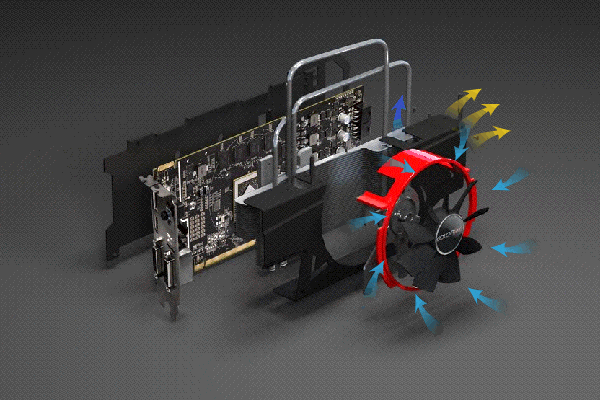
1. Micro-Fans (Internal Forced Convection)
Implementation: Integrating ultra-compact brushless fans (dimensions 15mm × 10mm × 5mm) directly inside the module.
Performance: High-speed operation (10,000 – 20,000 RPM) boosts cooling efficiency by 2-3 times compared to passive methods.
Critical Engineering: A Vibration Damping Structure is essential.
Expert Note: High-speed fans create micro-vibrations. Without isolation, this mechanical noise interferes with the Laser Diode (LD), causing signal jitter or optical misalignment.
2. Thermoelectric Coolers (TEC)
Target Application: Essential for highly temperature-sensitive components, such as Coherent Receivers or DWDM lasers.
Mechanism: Using miniature TEC chips (
≤5mm × 5mm) based on the Peltier effect.Capabilities: Provides Precision Temperature Control, capable of achieving a temperature differential of up to 50°C.
The Trade-off: TECs are active devices that consume power themselves (adding 10-20% extra overhead).
Thermal Challenge: You must simultaneously dissipate the heat from the component plus the heat generated by the TEC itself from its “hot side.”
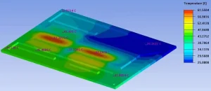
5. Thermal Simulation & Verification
The Rule of Engineering: You cannot jump straight from design to mass production. Potential failures must be predicted via Simulation, followed by optimization through physical Verification.
Phase 1: Thermal Simulation (CFD Analysis)
Using industry-standard CFD software like ANSYS Icepak or Flotherm to build detailed 3D models.
Setup Parameters:
Ambient Temperature: Simulation range covers -40°C to 85°C.
Heat Source Power: Input precise wattage based on component Datasheets (e.g., DSP at 10W, Laser Diode at 2W).
Boundary Conditions:
Simulate the switch environment: Airflow Velocity = 1 m/s.
Cage Heat Transfer Coefficient = 10 W/(m²·K).
Design Goals :
Junction Temperature : Must stay below rated limits (e.g., LD ≤85°C, DSP ≤105°C).
Case Temperature: Must remain ≤ 60°C to meet Touch Temperature Safety standards (preventing scalding).
Phase 2: Physical Verification (Testing)
Environmental Chamber Testing :
Test the module under varying temperatures and airflow conditions.
Tools: Use Thermocouples for contact measurement and IR Thermal Imagers to detect hotspot distribution.
Long-Term Reliability:
The “85/85” Test: Continuous operation for 1000 hours under 85°C temperature and 85% Relative Humidity (RH).
Criteria: Monitor for any drift in temperature stability or degradation in optical performance.
Thermal Management in Data Center Compute Clusters: Technology Classification & Core Requirements
The Power & Heat Surge:
Driven by the demand for higher bandwidth in AI and HPC clusters, optical transceivers are evolving rapidly from 400G to 800G and 1.6T. Consequently, power consumption is skyrocketing:
400G: ~10-15W
800G: ~25-35W
1.6T (Projected): >50W
These modules must operate reliably within High-Density Racks (power per rack >100kW) and under elevated ambient temperatures (Rack Inlet Temp: 25-40°C).
Core Thermal Management Challenges
1. Chip-Level Dissipation (Handling Extreme Heat Flux)
The Target: Laser Diodes (LD), Driver ICs, TIAs, and primarily the DSP (Digital Signal Processor).
The Challenge: Dealing with extreme Local Heat Flux Densities.
Expert Statistic: The heat flux of a modern 7nm/5nm DSP chip often exceeds 100W/cm². (To put this in perspective, that’s approaching the heat density of a nuclear reactor core, but on a micro scale).
2. Module-Level Thermal Spreading (Uniformity)
The Goal: Rapidly transferring heat from these tiny chips to the module’s outer casing (Housing).
The Criticality: Achieving Thermal Uniformity to prevent localized “Hotspots” that degrade performance while keeping the rest of the case cool.
3. System-Level Integration (Cooling Synergy)
The Context: The module must align with the rack’s cooling ecosystem (Air-Cooled or Liquid-Cooled).
The Limit: Ensuring the Junction Temperature never breaches component specs (e.g., LD
<90∘C<90∘C, DSP<105∘C<105∘C) even when the external environment is harsh.
Technology Classification & The Role of TIMs
Mainstream thermal management solutions fall into three categories: Passive Cooling, Active Cooling, and Hybrid Cooling.
The Pivot Point: Across all these architectures, Thermal Interface Materials (TIMs) act as the “Critical Junction” , bridging the gap between heat sources and dissipation structures.
Comparison of Mainstream Thermal Technologies & TIM Solutions
Cooling Modes of Optical Transceivers
1. Passive Cooling Technology (No Fan/TEC, Natural Convection & Conduction)
Technical Principle:
Relying on the physics of Thermal Conduction and Natural Convection. Heat is transferred from the chip to the module housing via high-conductivity materials (TIMs), and then dissipated into the environment via the airflow in the rack.
Target Application: Low-to-medium power modules (<20W) or noise-sensitive environments (e.g., Enterprise Data Centers).
Key Technical Pillars:
Chip Packaging: Replacing traditional FR4 (0.3 W/m·K) with High-Conductivity Substrates like Aluminum Nitride (AlN) Ceramics (170-200 W/m·K) to drastically lower the Chip-to-Substrate thermal resistance.
Thermal Interfaces:
Chip-to-Substrate: Using Gold-Tin (AuSn) Solder (57 W/m·K) or Silver Sintering (>200 W/m·K).
Substrate-to-Case: Filled with Thermal Grease (3-5 W/m·K) or Thermal Pads (5-10 W/m·K).
Housing Design: Using Aluminum/Copper Alloys (200-400 W/m·K) combined with Fins (to increase surface area), relying on the rack’s natural convection heat transfer coefficient (
h≈5−10W/m2⋅Kh≈5−10W/m2⋅K).
Typical TIM Solutions (Material Examples):
Thermal Grease:
Shin-Etsu X-23-7783D (3.5 W/m·K)
Dow Corning TC-5022 (4.5 W/m·K)
Thermal Pads:
Bergquist Gap Pad 4000S (10 W/m·K, High conformability)
Feirongda FP-G50 (Domestic solution, 8 W/m·K)
Phase Change Materials (PCM):
Honeywell PTM7950 (Changes phase at 50-70°C to fill micro-voids; Thermal Conductivity 5-6 W/m·K). Expert Note: PCM is currently the industry favorite for balancing reliability and performance.
2. Active Cooling Technology (Fan/TEC, Forced Convection or Active Refrigeration)
Technical Principle:
Enhancing dissipation capability via Micro-fans (Forced Air) or Thermoelectric Coolers (TEC).
Target Application: High-power modules (>25W, e.g., 800G/1.6T) or high-temperature environments (Rack Inlet Temp >35°C).
Key Technical Pillars:
Forced Air Cooling: Integrating micro-fans (e.g., 30mm diameter, 5-10 m/s velocity) into the module housing to create forced airflow. This boosts the heat transfer coefficient to 20-50 W/m²·K, keeping the case temperature between 60-75°C.
TEC (Peltier Cooling): Integrating a Peltier element between the chip and the heatsink case. It uses DC current to actively pump heat, achieving a of 50-70°C.
Trade-off: Consumes extra power (approx. 1-3W per module).
Thermal Interfaces:
TEC Cold Side: Must have tight contact with the chip using high-conductivity grease or metal sintering (Thermal Resistance
<0.5∘C⋅cm2/W<0.5∘C⋅cm2/W).TEC Hot Side: Dissipates heat via copper fins.
Typical TIM Solutions (Material Examples):
High-Performance Thermal Grease:
Arctic MX-6 (8.5 W/m·K, for Fan-cooled modules)
Shin-Etsu X-23-7921 (6 W/m·K, Optimized for TEC Cold Side application).
Metal Sintering Materials:
Indium Solder (80 W/m·K, critical for reliable TEC-to-Chip bonding).
Silver Nanoparticle Paste (>200 W/m·K, extremely high cost but peak performance).
Graphene Thermal Films:
Moorui Tech (Domestic, 1500-2000 W/m·K in-plane conductivity, Ultra-thin <0.1mm).
3. Hybrid Cooling Technology( Passive + Active Synergy)
Technical Principle:
Combining the foundational efficiency of passive conduction with the boosted capacity of active cooling to balance cost and performance.
Scenario 1: 800G Module using AlN Substrate + Phase Change TIM (Passive foundation) + Edge Micro-fan (Active boost).
Scenario 2: DSP Chip integrated with a localized TEC (Active spot cooling) + Outer Case Fins (Passive dissipation).
Next Up: Thermal Design Priorities for Different Module Speeds
Thermal Design Evolution by Module Speed & Form Factor
| Module Type / Form Factor | Typical Power (W) | Dimensions (mm) | Core Thermal Strategies |
| 100G QSFP28 | 5 – 8W | 18.3 × 56.5 × 13.6 | • Heavy Copper PCB• Thermal Silicone Pad• Anodized Aluminum Housing |
| 400G QSFP-DD | 12 – 15W | 18.3 × 76.2 × 13.6 | • Embedded Copper Coin • Internal Metal Bracket • Cage Interface Optimization |
| 800G OSFP | 20 – 30W | 39.4 × 78.0 × 18.5 | • Micro-fan • TEC (Thermoelectric Cooler)• High-Performance TIM |
As data rates evolve towards 1.6T and 3.2T, power consumption is poised to breach the 50W threshold. This demands a paradigm shift in thermal engineering beyond traditional methods:
1. Material Innovation: The Graphene Revolution
Strategy: Replacing traditional copper foils with Graphene Thermal Films.
The Advantage: With a staggering thermal conductivity of 1500 – 5000 W/(m·K) (compared to Copper’s ~400 W/(m·K)), graphene offers an Ultra-thin Profile combined with superior heat spreading efficiency, critical for squeezing into tight spaces.
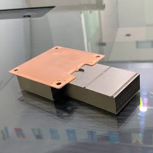
2. Structural Innovation: Full Metal Packaging
Strategy: Adopting a “Full Metal Packaging” architecture.
The Mechanics: Bonding the PCB and high-heat chips directly to the metal housing/shell. This minimizes the thermal path length and eliminates intermediate interfaces, thereby Maximizing Conduction Efficiency.
3. System Synergy: Holistic Co-Design
Strategy: Moving from isolated component design to a collaborative Module-Switch Co-Design approach.
The Implementation: Features like Integrated Cage Fins (heatsinks built into the connector cage) and targeted Airflow Optimization (channeling air precisely where needed).
The Goal: Establishing a unified “Module-Cage-Switch” integrated thermal ecosystem.
1.Application Scenarios
Optical Chip to Baseplate:
Adopt Thermal Silicone Pads with Thermal Conductivity≥6W/m⋅K≥6W/m⋅KGoal: Rapidly conduct heat from the chip to the metal housing/baseplate.
Laser to TEC (Thermoelectric Cooler):
Use Phase Change Materials (PCM).Mechanism: Absorbs peak heat loads through the physical process of melting and solidifying (Phase Transition), ensuring temperature stability.
PCB to Housing:
Fill with Thermal Gel.Goal: Eliminate localized Hotspots on the board.
2. Key Selection Criteria
Thermal Conductivity: Prioritize materials with
≥3W/m⋅K≥3W/m⋅K.Thickness Tolerance: Control within
±0.05mm±0.05mm.Expert Note: This precision is vital to prevent excessive assembly pressure from deforming the delicate optical alignment.
Compression Set:
≤10%≤10%(per ASTM D575 Standard).Significance: Ensures long-term reliability and contact integrity after repeated thermal cycling.
Temperature Range: -40°C to 150°C.
Requirement: Must withstand extreme industrial and outdoor environments.
TIM Solutions by Module Type
For 400G Optical Modules:
The Challenge: High heat generation from the chipset.
The Solution: Requires Thermal Gel with Conductivity
>6W/m⋅K>6W/m⋅K.The Benefit: Improves overall thermal dissipation and maintains the stability of the Optical Path.
For 800G High-Power Modules:
The Challenge: Extreme power consumption (typically 20-30W).
The Solution: Industry recommendation is High-Performance Thermal Gel with
≥7.5W/m⋅K≥7.5W/m⋅K.Industry Examples:
Parker Chomerics GEL75 (
7.5W/m⋅K7.5W/m⋅K)
Hanhua KG100TG (
10W/m⋅K10W/m⋅K)
The Goal: Ensuring rapid heat extraction from high-power components like the DSP, preventing thermal throttling.
Thermal Material Selection Reference for 1.6T Optical Transceivers
| Target Component | Core Requirements | Recommended Material Type | Key Performance Specs (Thermal Conductivity) |
| TOSA (Laser) | High Conductivity, Low Stress, High Stability | High-Performance Thermal Gel | |
| ROSA (Receiver) | Low Bleed/Outgassing, Ensure Clean Optical Interface | Low-Bleed Thermal Pad | Approx. |
| DSP / Driver IC | Ultra-High Conductivity, Rapid Heat Extraction | Graphene Thermal Pad | Through-Plane Conductivity |
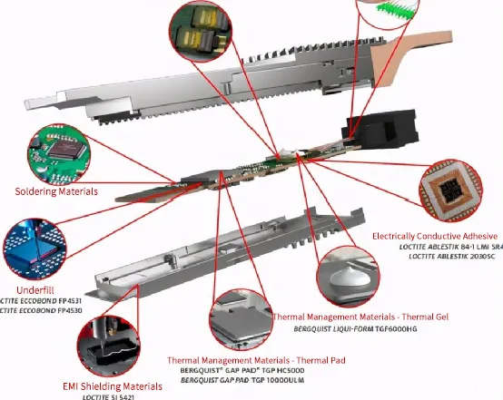
Thermal Management Materials Market for Optical Modules
Estimation Example: TIM Usage Calculation for an Optical Transceiver
1. Assumptions
DSP Chip Dimensions:
20mm×20mm=400mm220mm×20mm=400mm2Recommended Coverage Rate: 80%
(Considering material Squeeze-out and spreading during assembly )Effective Application Area:
400mm2×80%=320mm2400mm2×80%=320mm2Designed Bond Line Thickness (BLT): 0.2 mm
2. Calculation
Volume Calculation:
Volume=Area×ThicknessVolume=Area×ThicknessVolume=320mm2×0.2mm=64mm3Volume=320mm2×0.2mm=64mm3Mass Estimation:
Since1cm3=1mL1cm3=1mL, and assuming the TIM density is approx. 1 g/cm³:
64mm3=0.064cm3≈0.064g64mm3=0.064cm3≈0.064g
3. Conclusion
This implies that for the DSP chip alone, approximately 0.064g of TIM is required.
If a 1.6T Optical Transceiver contains 3 major heat sources (e.g., 1 DSP + 2 Optical Engines), the total TIM usage per module would likely range from 0.15g to 0.3g.
Chart: Demand Forecast for Thermal Materials by Optical Transceiver Type
| Module Type | 2025 Volume<br>(10k Units) | Share | Gel Usage(kg) | 2026E Volume(10k Units) | Share | Gel Usage(kg) | 2027E Volume(10k Units) | Share | Gel Usage(kg) |
| 400G | 1,500 | 40% | 4,500 | 600 | 10% | 1,800 | 170 | 2% | 510 |
| 800G | 2,000 | 53% | 6,000 | 4,500 | 76% | 13,500 | 4,950 | 72% | 14,850 |
| 1.6T | 250 | 7% | 750 | 800 | 14% | 2,400 | 1,800 | 26% | 5,400 |
| Total | 3,750 | 100% | 11,250 | 5,900 | 100% | 17,700 | 6,920 | 100% | 20,760 |
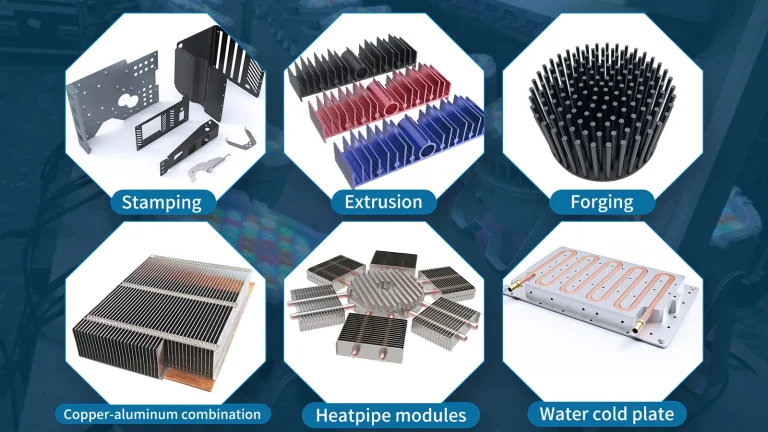
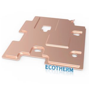
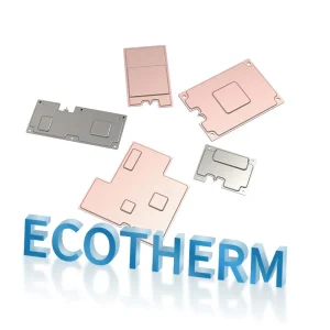
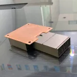
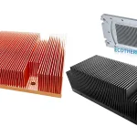
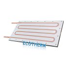
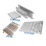
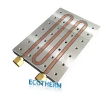
Ecothermgroup specialize in custom heat sinks, providing solutions for high-power cooling challenges.
We offer free, fast analysis and evaluation, with a commitment to responding within 24 hours.
Let us deliver the optimal cooling solution for your equipment.