Semiconductor Heat Dissipation Challenges
Semiconductors are increasingly constrained by heat, and effective design solutions are essential to mitigate and dissipate this heat.
The power consumed by semiconductors generates heat, which must be expelled from the device, but doing this effectively is becoming an increasingly difficult challenge.
Heat is a byproduct of semiconductor operation. This phenomenon occurs as power dissipates in the device and its wiring. Devices consume power when switching, meaning the process is activity-dependent. Imperfect devices and wiring continuously waste power, and design flaws can lead to unnecessary heat generation. At times, design teams must figure out how to eliminate this heat, as failure to do so will drastically shorten the product’s lifespan.
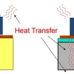
There are only three processes that control heat transfer: conduction, convection, and radiation. In simple terms, conduction applies to solids, convection to liquids and gases, and radiation to vacuums, a scenario rarely seen in semiconductors.
“The three steps involved in heat are generation, conduction, and dissipation,” said Marc Swinnen, Marketing Director of Ansys’ Semiconductor Division. “You generate heat, conduct it somewhere, and then dissipate it. Power analysis tells you where the heat is generated. Conduction and dissipation are physical analyses that involve fluid dynamics. All three must be included in system analysis because they have feedback on each other.”
As transistor density increases, this challenge becomes even more significant. “Most people can change the conduction path,” said Karthick Gopalakrishnan, Thermal Solver Product Engineer at Cadence’s Multiphysics Systems Analysis Group. “Materials and design improvements can help conduct more heat away with heat sinks. The challenge is that unless we’re using large servers, the heat space around these devices is very small. You must consider material improvements, chips, packages, or smart utilization of the thermal space around the PCB. What you really want is to increase the conduction heat transfer rate.”
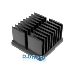
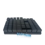
However, simply adding a large heat sink to a device without proper analysis can lead to other issues. It’s necessary to consider airflow and the mechanical design of the surrounding space to assess the effects on other components.
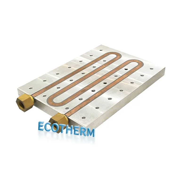
Even heat sinks themselves have limitations. “There are many ways to eliminate heat from a system, such as forced liquid cooling,” said William Ruby, Product Manager at Synopsys EDA Group. “We’ve seen some advanced packaging make significant progress. With 3D-IC design, forced airflow and liquid cooling are used. New concepts, such as special vias to reduce heat and help disperse it, are also emerging.”
Unlike the vast differences in electrical conductivity between conductors and insulators, thermal conductivity is limited to a certain extent. “The thermal conductivity of silicon is between 100 and 120 watts per meter Kelvin (W/(m·K)), which is already quite good for a heat-conductive material,” said John Parry, Director of Electronics and Semiconductor Industries at Siemens Digital Industries Software’s Simcenter Product Portfolio. “Copper has a thermal conductivity of 400, and copper is often used as the best economic heat conductor.” Other economic factors also come into play. Javier DeLaCruz, Senior Director and Researcher at Arm’s Systems Integration and Development Division, stated: “The main cost drivers in data centers are not the cost of heat dissipation methods but the operational costs associated with managing thermal transfer at a data center level. The power entering a data center is limited, and this power is shared between powering computing systems and dissipating heat. Therefore, performance per watt must be a key focus, not just performance.”
Heat can significantly impact performance. “Even with the best heat dissipation strategies, each chip will heat up to varying degrees during circuit operation, reducing performance,” said How-Siang Yap, Product Manager at Keysight EDA. “Dynamic temperatures can change the electrical characteristics of a device, such as gain, impedance, load mismatch, and more advanced waveform characteristics like error vector magnitude (EVM) and adjacent channel leakage ratio (ACLR) in RF circuits with digital modulation signals. In analog systems, the performance penalty can be even higher.”
Analyzing heat dissipation is not simple. “Today’s chips are so complex that it’s hard to define how to create activities that can show the worst-case conditions,” said Swinnen from Ansys. “When you look at timing errors caused by temperature, you’re dealing with nanoseconds, or at most, a few microseconds. Also, the time constants for electrical and thermal parameters differ by at least two orders of magnitude. When heat dissipates, it slowly spreads through the chip and neighboring areas, so the heat increase you observe may be due to something that happened two seconds ago elsewhere.”
Heat Distribution Within the Chip
Heat tends to spread in all directions. “You can’t truly stop heat from flowing anywhere,” said Parry from Siemens. “You can guide it, but that’s very different from the electrical world, where the conductivity differences between conductors and insulators can be 20 or 21 orders of magnitude. In the electrical world, you can direct current where you want it, but thermally, you cannot do the same.”
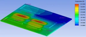
Since heat depends on activity, the temperature across the chip’s surface is neither constant nor evenly distributed. “You may have a hotspot created by parts of the design that involve heavy computational tasks, such as hardware accelerators,” said Ruby from Synopsys. “Other parts of the chip may be less active or used only in specific operating modes. Temperature gradients on the chip depend on workload or activity.”
While heat dissipation is theoretically simple, it becomes much more complex in practice. “You want to spread heat as much as possible across layers to minimize hotspots,” said Gopalakrishnan from Cadence. “You must consider where things are placed. Moving certain components to the edge of the chip is not always feasible, as heat doesn’t always diffuse in one direction at the edges.”
Effective Design Solutions
In theory, a custom heat sink can help manage heat, but practical implementation involves many variables. “Using thermal-aware floorplanning and layout of components is one effective technique,” said Ruby. “The basic idea is to arrange components to minimize peak temperatures and temperature gradients. With physical-aware RTL power analysis tools, you can analyze the initial layout and then input the power curve data into thermal analysis. This analysis can take place earlier, reducing the need for last-minute changes.”
For large heat sink applications, especially with 3D-ICs, better TSV (Through-Silicon Vias) placement can assist with heat dissipation, but limitations still exist due to valuable space constraints and local efficiency. “Better TSV placement helps, but it is limited because they occupy valuable space,” said Gopalakrishnan. “However, they can be useful when targeting hotspots near chips or power blocks.”
Conclusion
Many chips face thermal challenges, and solving these problems is not easy. “Unfortunately, heat is a limiting factor for integration density,” said Swinnen. “We can design and manufacture incredible chips, but they melt due to excess heat. This is not a manufacturing or design limit—it’s a physical limit. We cannot dissipate more heat.”
Despite some unique solutions in certain applications, most markets must find ways to do more with fewer resources, meaning more functionality per watt. The cost associated with this challenge is significantly higher than past solutions.