Cold Plate Design Guide (Part 2): Thermal Calculation for Optimal Performance
Introduction
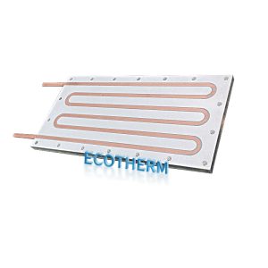
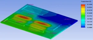
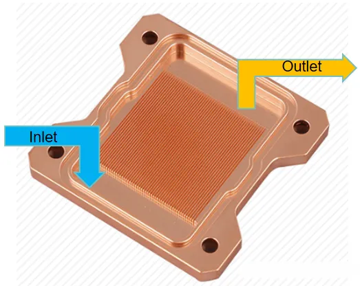
This section will provide a detailed explanation of how to calculate the thermal performance of cold plates, based on the formulas presented in the foundational section of cold plate design. All calculations are based on a flat-channel scalloped microgroove cold plate, as shown in Figure 1.
The calculations are based on the thermal properties of copper (Cu), with a thermal conductivity of K = 385 W/mK. The coolant used is PG25, and the properties at 45°C are obtained through linear interpolation as follows:
Density (ρ) = 1014.9 kg/m³
Specific heat capacity (Cp) = 3972 J/kg·K
Thermal conductivity (k) = 0.481 W/m·K
Viscosity (μ) = 1.245 mPa·s
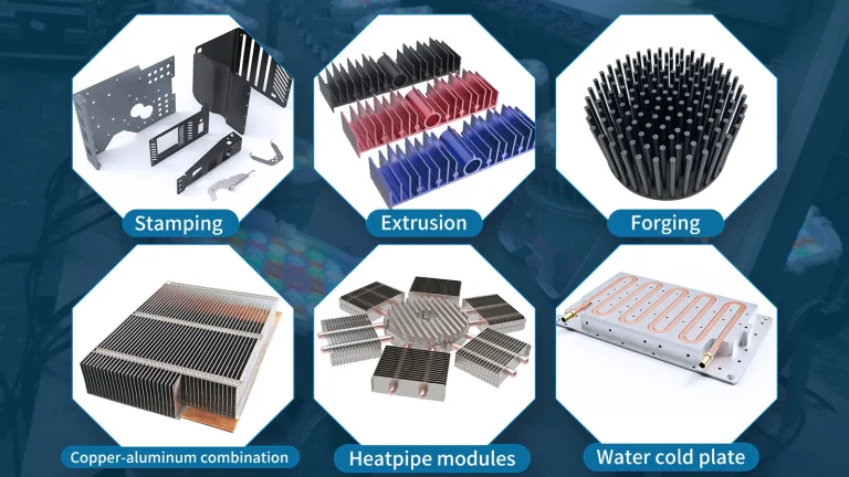
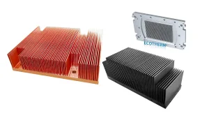
1. Scalloped Fin Process Selection and Parameters
1.1 Mainstream Cold Plate Structure
Application Scenario: Cooling for high-power chips such as GPU, CPU, ASIC, etc.
Typical Structure: Parallel channel design, where the coolant flows in from one side, exchanges heat through the fin area, and exits from the other side (Figure 1).
Simplified Structure Conditions: If the thickness of the substrate and cover plate is sufficient (to meet pressure tolerance), reinforcing ribs may not be necessary.
1.2 Process Capability Comparison
| Parameter | Mainstream Level | Advanced Level |
|---|---|---|
| Finning Capacity | Fin thickness 0.1mm, gap 0.1mm | Fin thickness 0.05mm, gap 0.05mm |
| Substrate Thickness | 2 – 3mm | 1mm (pressure – resistant structure required) |
| Welding Process | Brazing / Friction Stir Welding | Transient Welding of the Same Metal |
| Total Cold Plate Height | 15 – 20mm | ≤12mm (10mm at extreme) |
2. Fin Area Size Design
2.1 Design Principles
Substrate Characteristics: The copper cold plate substrate is thin (δ = 2-3mm), and the lateral heat resistance is greater than the convective heat resistance of the fins.
Fin Area Size Formula:
Chip Size: Length × Width = L1 * W1
Fin Area Size:
L2 = L1 + 2 * δ
W2 = W1 + 2 * δ
2.2 Special Case Handling
Uniform Power Consumption: Designed according to the formula mentioned above.
Non-Uniform Power Consumption: Customize the fin area based on the chip power distribution diagram.
Size Constraints: The fin area must be ≥ the chip size (L2 ≥ L1, W2 ≥ W1), and it is not allowed to be smaller than the chip size.
3. Thermal Calculation Case Analysis
3.1 Boundary Conditions
| Parameter | Value |
|---|---|
| Chip Power Consumption | 750W |
| Chip Size | 25mm × 30mm |
| Chip Power Density q | 100 W/cm² |
| Case Temperature Limit Tc | 80°C |
| Cooling Fluid | PG25 (Inlet 40°C, Outlet 52°C) |
3.2 Thermal Resistance Target Decomposition
| Temperature Rise Item | Symbol | Calculated Value | Formula/Basis |
|---|---|---|---|
| Total Allowable Temperature Rise | ΔT | 40K | Tc−Tin |
| TIM Layer Temperature Rise | ΔT1 | 6K | q×Rtim (Rtim=0.06 K⋅cm2/W) |
| Allowable Temperature Rise of Cold Plate Bottom Surface | ΔT2 | 34K | ΔT−ΔT1 |
3.3 Substrate Temperature Rise Calculation
The relationship between substrate thickness δ and temperature rise (ignoring lateral heat conduction) is as follows:
δ = 3mm: 7.8 K
δ = 2mm: 5.2 K
ΔTbase ∝ δ
Conclusion: For every 1mm reduction in substrate thickness, the temperature rise decreases by approximately 2.6K (@ 100W/cm²).
3.4 Microgroove Area Heat Transfer Analysis
Flow Characteristics
(For a cross-sectional area of 31 * 4mm, the flow velocity is calculated as V = 0.25 m/s):
| Fin Thickness (mm) | Fin Spacing (mm) | Fin Height (mm) | Equivalent Hydraulic Diameter of Fin (mm) | Re | Length of Inlet Section (mm) |
|---|---|---|---|---|---|
| 0.2 | 0.2 | 4 | 0.38 | 77.64 | 1.48 |
| 0.3 | 0.3 | 4 | 0.56 | 113.75 | 3.17 |
The flow between the fins is laminar, and the entrance section is much smaller than the channel length. Therefore, the flow between the fins is fully developed laminar flow.
In the fully developed laminar flow region, the Nusselt number (Nu) is constant. When the channel aspect ratio (length-to-width) is greater than 8, Nu = 6.49.
Under these conditions, the microgroove fin data for two different fin parameters are as follows, from which the relative temperature rise of the coolant on the upper surface of the cold plate substrate can be estimated.
| Fin Thickness (mm) | Fin Spacing (mm) | Fin Height (mm) | Equivalent Hydraulic Diameter of Fin (mm) | h (W/m²K) | Fin m | mH | Fin Heat Transfer Efficiency η | Equivalent Fin Height Heff (mm) |
|---|---|---|---|---|---|---|---|---|
| 0.2 | 0.2 | 4 | 0.38 | 8194.44 | 461.35 | 1.85 | 0.52 | 2.06 |
| 0.2 | 0.2 | 6 | 0.39 | 8064.37 | 457.67 | 2.75 | 0.36 | 2.17 |
| 0.3 | 0.3 | 4 | 0.56 | 5593.03 | 311.21 | 1.24 | 0.68 | 2.72 |
| 0.3 | 0.3 | 6 | 0.57 | 5462.96 | 307.57 | 1.85 | 0.52 | 3.09 |
| Fin Thickness (mm) | Fin Spacing (mm) | Fin Height (mm) | Equivalent Fin Height Heff (mm) | Total Convective Thermal Resistance in Microchannel Region (cm²K/W) | Temperature Rise at 100W/cm² Heat Flux Density (K) |
|---|---|---|---|---|---|
| 0.2 | 0.2 | 4 | 2.06 | 0.11 | 10.79 |
| 0.2 | 0.2 | 6 | 2.17 | 0.10 | 10.48 |
| 0.3 | 0.3 | 4 | 2.72 | 0.18 | 17.75 |
| 0.3 | 0.3 | 6 | 3.09 | 0.16 | 16.18 |
3.4 Estimation of Overall Temperature Rise of the Cold Plate
| Total Power Consumption of Chip (W) | TIM Thermal Resistance (cm²K/W) | Thickness of Substrate (mm) | Fin Parameters | Temperature Difference Between Inlet and Outlet Fluid (K) | Temperature Rise of Substrate (K) | Temperature Rise of Fin Convection (K) | Total Temperature Rise of Cold Plate Hot Spot (K) |
|---|---|---|---|---|---|---|---|
| 750 | 0.06 | 3 | Thickness 0.2, Spacing 0.2, Height 4 | 12 | 7.8 | 10.79 | 30.59 |
| 750 | 1.06 | 4 | Thickness 0.2, Spacing 0.2, Height 6 | 12 | 8.8 | 10.48 | 31.28 |
| 750 | 2.06 | 5 | Thickness 0.3, Spacing 0.3, Height 4 | 12 | 9.8 | 17.75 | 39.55 |
| 750 | 3.06 | 6 | Thickness 0.3, Spacing 0.3, Height 6 | 12 | 10.8 | 16.18 | 38.98 |
Note: The actual maximum temperature is slightly lower than the calculated value (due to the exclusion of lateral heat conduction effects in the substrate).
4. Design Summary and Key Conclusions
4.1 Process Selection Priorities
Fin Gap:
Recommended ≥ 0.15mm (to prevent clogging).
Substrate Thickness:
Preferred ≤ 2mm (temperature rise decreases by approximately 2.6K/mm).
Scalloped Ability:
Mainstream level (0.1mm thick/gap) meets the requirements, and there’s no need to pursue 0.05mm.
4.2 Size Design
Minimum Fin Area Recommendation:
L2 = L1 + 2δ, W2 = W1 + 2δ (where δ is the substrate thickness).
Restricted Zone:
The fin area must be ≥ chip size (otherwise, the risk of local overheating increases significantly).
4.3 Thermal Optimization Key Factors
Fin Parameters:
Thickness/Gap = 0.2mm/0.2mm results in a temperature rise reduction of nearly 7K compared to 0.3mm/0.3mm (at the same height).
Fin height has minimal impact (changing from 4mm to 6mm results in only a 0.3K temperature drop).
Flow Rate Control:
Maintain a flow velocity < 0.25 m/s to ensure fully developed laminar flow (Re < 2300).