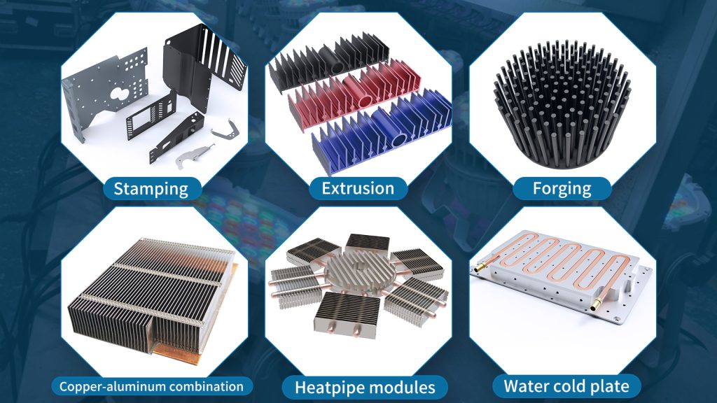
Heat Sink Solutions:Other Cooling Technologies (Diamond and Graphene Cooling)
Diamond Cooling
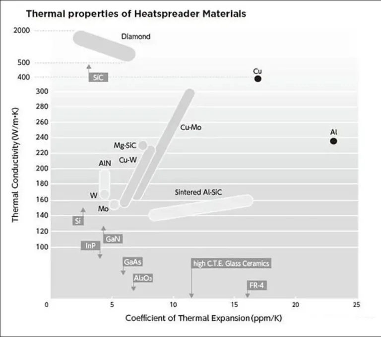
Diamond has one of the highest known thermal conductivities, reaching 2000 W/m·K, which is 13 times that of silicon (Si), 4 times that of silicon carbide (SiC), 43 times that of gallium arsenide (GaAs), and 4–5 times that of copper and silver. When the required thermal conductivity ranges from 10 to 200 W/(m·K), diamond is the only viable heat sink material.
The thermal conductivity of diamond is as high as 1000–2000 W/m·K.
The thermal conductivity of diamond is as high as 1000–2000 W/m·K.
In November 2024, the diamond cooling technology developed by Akash Systems in the United States can reduce the temperature of GPUs by 20 degrees and increase the overclocking potential by 25%. Therefore, it has signed a non – binding memorandum of preliminary terms (PMT) with the US Department of Commerce and will receive $18.2 million in direct funding and $50 million in federal and state tax credits under the CHIPS and Science Act.
Nvidia, the global leader in GPU chips, has also started to use diamond – cooled GPUs for testing experiments. According to the official website of Diamond Foundry, Nvidia’s diamond – cooled GPUs can triple the performance of AI and cloud computing.
In addition, Huawei has conducted in-depth research in the field of diamond cooling and published multiple patents.
In 2014, Huawei’s technical team and Professor Yu Daquan’s team from the College of Electronic Science and Technology at Xiamen University published a research achievement titled “Low-Temperature Bonding Technology of Diamond Based on Reactive Nano-Metal Layers” in the Journal of Materials Science & Technology.
In 2014, Huawei’s technical team and Professor Yu Daquan’s team from the College of Electronic Science and Technology at Xiamen University published a research achievement titled “Low-Temperature Bonding Technology of Diamond Based on Reactive Nano-Metal Layers” in the Journal of Materials Science & Technology.
In October 2023, Huawei and Harbin Institute of Technology jointly applied for and disclosed a patent titled A Hybrid Bonding Method for Three-Dimensional Integrated Chips Based on Silicon and Diamond. By adopting a hybrid bonding method, this technology enables efficient integration of silicon and diamond, rapidly (conducts out) heat generated by the chip, reduces thermal resistance, and thus improves the chip’s heat dissipation efficiency, performance, and reliability.
In December 2024, Huawei applied for and disclosed a patent for a semiconductor device using a diamond heat dissipation layer. In this semiconductor device, a passivation layer is positioned between the first epitaxial layer and the diamond heat dissipation layer. The surface of the passivation layer facing the diamond heat dissipation layer is provided with grooves. This structure not only increases the contact area between the diamond heat dissipation layer and the passivation layer, thereby enhancing the bonding force between them, but also reduces the thermal diffusion distance along the thickness direction of the semiconductor device between the gate and the diamond heat dissipation layer, significantly improving the heat dissipation efficiency of the semiconductor device.
Diamond can also be mixed with metals such as copper and aluminum to produce materials like diamond-copper and diamond-aluminum, with thermal conductivity exceeding 800 W/(K·m). These materials can be prepared using the MIM (Metal Powder Injection Molding) process.
Graphene Cooling Technology
Graphene is a two-dimensional material with a single-atom-thick layer, exhibiting extremely high thermal conductivity. In 2008, the Balandin research team first measured the thermal conductivity of single-layer graphene using Raman spectroscopy and observed that its thermal conductivity could reach up to 5300 W/m·K, higher than that of bulk graphite and diamond. This represents the highest known thermal conductivity among materials, attracting extensive attention from researchers.
Studies on the thermal conductivity of graphene quickly inspired its applications in the field of heat conduction. With the development of large-scale graphene preparation technologies, highly thermally conductive graphene films prepared via the graphene oxide method can achieve a thermal conductivity of ~2000 W·m⁻¹·K⁻¹. These films are comparable to high-quality graphitized polyimide films used in industrial applications, while offering lower costs and better thickness controllability. On the other hand, as a two-dimensional thermal conductive filler, graphene easily constructs three-dimensional thermal conductive networks in polymer matrices, showing promising applications in thermal interface materials. By improving the dispersibility of graphene in polymer matrices and constructing three-dimensional graphene thermal conductive networks, the thermal conductivity of graphene-filled thermal interface composites can be increased by several times compared to pure polymers, with filler ratios lower than those of traditional thermal conductive fillers.
Thus, whether used as self-supporting thermal conductive films or as thermal conductive fillers in thermal interface materials, graphene will play a significant role in heat dissipation applications for electronic components.
>>>Heat Sink Solutions: Scaling for Data Centers and Chip Evolution
>>>Heat Sink Solutions:Development of Data Centers
>>>Heat Sink Solutions:Vapor Chamber (VC) Cooling Technology
>>>Heat Sink Solutions:3D VC (Three-dimensional two-phase Homogeneous Temperature technology)
>>>Heat Sink Solutions:Liquid cooling heat dissipation technology
>>>Heat Sink Solutions:Other Cooling Technologies (Diamond and Graphene Cooling)
>>>Heat Sink Solutions:Heat Dissipation Path and Development Route of Thermal Interface Materials