Thermal Characteristics & Optimization Design of Aerospace PCBs
Ready to optimize your thermal design?
Send us your STEP files or thermal requirements today, and our engineers will provide a complimentary thermal feasibility review within 24 hours.
Abstract
This paper establishes a heat transfer model for a specific satellite printed circuit board (PCB) to investigate its temperature field under a preliminary thermal design. Furthermore, an optimization design is proposed to address the thermal management of high-power, overheating components on the PCB.
ANSYS software is utilized to simulate the operational temperature field of the board. Based on thermal resistance theory, a passive thermal control optimization strategy is implemented. This involves welding thermally conductive copper strips to directly connect the components to the equipment chassis, thereby enhancing heat conduction and lowering component temperatures.
An analysis of the high-power devices’ temperature variations before and after the optimization reveals that the integration of copper strips effectively reduces their operating temperatures. The results indicate that combining ANSYS simulations with thermal resistance theory for passive thermal control optimization—specifically via copper strip-to-chassis connections—yields significant improvements in cooling high-power components. This approach provides a practical reference for the thermal design of satellite PCBs. Future research will explore the applicability and further optimization potential of this method across various operating conditions and component layouts.
Introduction
With the rapid development of the aerospace industry, China has launched various types of spacecraft, including space stations, manned spacecraft, cargo spacecraft, space probes, and artificial satellites. In recent years, in particular, the market demand for diverse satellite applications has continued to grow. Against this backdrop, the rapid advancement of aerospace technology has imposed stricter requirements for the optimization and improvement of thermal designs for printed circuit boards (PCBs) in onboard equipment.
The versatility of satellites heavily relies on the coordinated operation of various onboard devices. As the functional capabilities and lifespan requirements of satellite equipment increase, the power dissipation of electronic components rises significantly. Concurrently, the reduction in physical size and the higher density of spatial layouts make ensuring the reliable operation of these chip-level components increasingly critical.
Among all the components populated on a PCB, high-power components act as the critical units that determine whether the satellite equipment can operate reliably and effectively. The operational nature of these high-power components dictates that their working temperatures will inherently be higher than those of standard components.
Research indicates that the performance of electronic components is highly sensitive to temperature, with thermal overstress being the primary failure mode (accounting for 55% of all failure causes). When the operating temperature exceeds 80°C, component reliability degrades by approximately 10% for every 2°C increase.
Consequently, the thermal management of specific high-power components presents a prominent challenge: if heat cannot be dissipated promptly, the operating temperature will exceed allowable limits, leading to component or even complete equipment failure, which ultimately compromises the lifespan and reliability of the entire satellite system.
Therefore, implementing effective PCB thermal design for onboard satellite equipment is a critical step in ensuring the quality and reliability of aerospace electronics. Since evaluating the rationality of PCB thermal designs through empirical testing is highly time-consuming, this paper utilizes ANSYS software to simulate the PCB temperature field of a specific onboard device. The study investigates the temperature distribution of the PCB after a preliminary thermal design is subjected to a simulated space environment, and proposes an optimized design specifically targeting the heat dissipation of high-power components.
1. Theoretical Basis
Satellite electronic equipment operates in harsh space environments characterized by high vacuum, weightlessness, and intense solar radiation. Consequently, its thermal design requirements differ significantly from those of terrestrial and aeronautical electronics.
Because spaceborne equipment is exposed to a vacuum environment, convective cooling paths are absent. Therefore, spaceborne electronic devices rely primarily on heat conduction and thermal radiation for heat dissipation.
In this paper, conductive heat dissipation refers to the process where heat generated within power components is first conducted to the PCB, and then further transferred through the PCB to the equipment chassis. Thermal radiation exists between all components within the device that have a temperature above 0 K.
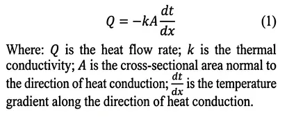
The heat conduction process is governed by Fourier’s law of thermal conduction, expressed as:
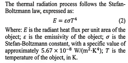
As the primary method of heat dissipation, thermal conduction is the core focus of this analysis. Based on the principle of thermal resistance, the heat conduction process in this study is analyzed, yielding the thermal resistance network diagram shown in Figure 1.
As illustrated in Figure 1, the silicon chip utilized in this specific spaceborne equipment acts as the sole internal heat source. The heat it generates dissipates through two distinct mechanisms:
A portion is transferred directly from the chip casing to the chassis via radiative heat exchange.
Another portion is conducted through the chip casing or pins to the PCB, and subsequently conducted to the chassis.
Ultimately, the heat radiates outward through the chassis exterior, completing the thermal dissipation to the external space environment. It is also important to note that continuous radiative heat exchange occurs simultaneously among the various internal sections of the chassis itself.
In a vacuum environment, the complete absence of air convection dictates that no convective heat transfer can occur on the exterior surfaces of the chip. Consequently, thermal management between the chip and the chassis housing relies entirely on two parallel heat dissipation paths:
Path 1 (Thermal Conduction): Heat is transferred through the chip pins or casing into the PCB, which then conducts the thermal load directly to the chassis.
Path 2 (Thermal Radiation): Direct radiative heat exchange occurs constantly between the chip, the PCB, and the equipment chassis.
Together, these two parallel pathways jointly manage the entire thermal dissipation workload of the high-power chip.
2. Simulation Model Development
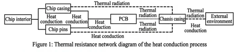
2.1 Equipment Structural Parameters
The external dimensions of the spaceborne equipment chassis in this simulation are 199 mm × 291 mm × 129 mm. The chassis is constructed from a specialized aluminum-magnesium alloy, featuring the following key thermal properties:
Heat Capacity: 4000 J/K
Surface Emissivity ($\varepsilon$): 0.8
Thermal Conductivity: 236 W/(m·K)
The overall equipment structure is illustrated in Figure 2.
2.2 Enhanced PCB Structure
The internal equipment consists of four circuit boards: a main signal board and its corresponding backup board, alongside a main processing board and its corresponding backup board. The dimensions of each circuit board are 144 mm × 285 mm × 1.6 mm.
Although standard PCB substrates possess excellent electrical and manufacturing properties, their thermal dissipation performance is relatively poor. This makes them highly susceptible to localized overheating when populated with high-power components. To address this, materials with superior thermal conductivity can be integrated into the PCB to improve overall heat transfer efficiency.
The PCB utilized in this simulation employs a multi-layer design. To explicitly enhance its thermal conduction capabilities, internal copper cladding layers are incorporated into the board structure. The specific parameters of this enhancement are:
Total Copper Thickness: 70 μm
Single-Layer Thickness: 17.5 μm
This structural enhancement significantly improves the PCB’s thermal conductivity, effectively mitigating the risks of localized overheating to a certain extent.
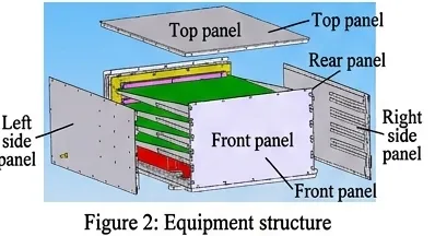
3. Computational Model
3.1 Material Specifications
Based on the equipment’s parameter information, a corresponding computational model is established to simulate the temperature distribution of the PCB under specific conditions. The structure of the developed model is illustrated in Figure 3.
The engineering data sources within the ANSYS software provide an extensive material database, allowing specific material parameters to be modified as required. For this simulation, the core materials and their respective thermal conductivities are defined as follows:
PCB Substrate (FR-4 Epoxy Glass Fiber): 0.38 W/(m·K)
Chip Material (Silicon – Si): 154.3 W/(m·K)
Packaging Material (Ceramic): 3.0 W/(m·K)
Chip Pins & Copper Cladding (Copper – Cu): 397.6 W/(m·K)
3.2 Contact Thermal Resistance
In the actual heat transfer process, thermal conduction between equipment components must account for contact thermal resistance.
To simulate this accurately, this study models the interface as a thin layer, assuming its thermal conductivity is governed by factors such as interfacial material properties and contact pressure. To ensure simulation precision, the mesh of these thin-layer models is refined during subsequent calculations.
The focus is placed on two critical connection interfaces: between the chip casing and the PCB, and between the PCB and the chassis housing. Thin-layer models are established at these junctions, with specific thermal resistance values assigned to each interface. These values are derived from previous experimental data and typical values found in relevant literature, ensuring they accurately reflect the thermal resistance of the respective materials under matching or similar temperature and pressure conditions.
With an estimated maximum experimental temperature reaching up to 200°C, the specific contact thermal resistance values are defined as follows:
Chip-to-PCB Interface: 0.01 K/W
PCB-to-Chassis Interface: 0.2 K/W
3.3 Component Parameters
The total power dissipation of the components distributed across the four internal circuit boards is detailed in Table 1.
Cumulatively, this results in a total equipment power consumption of 52.6 W.
Table 1
| Parameter | Parameter Value |
| Total power of the 1st layer circuit board | 3.6 |
| Total power of the 2nd layer circuit board | 22.7 |
| Total power of the 3rd layer circuit board | 3.6 |
| Total power of the 4th layer circuit board | 22.7 |
Given the elevated power levels of Layer 2 and Layer 4, it is reasonable to deduce that the maximum internal temperature of the equipment will manifest on these two specific circuit boards.
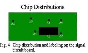
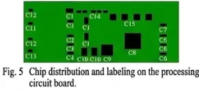
Figure 4 and Figure 5 illustrate the chip layouts for the signal circuit board and the processing circuit board, respectively. It should be noted that the chip layouts and all associated thermal parameters are strictly identical between the main boards and their corresponding backup boards.
The specific board configuration within the 4-layer stack is defined as follows:
Signal Circuit Boards: Layer 1 (Main Board) and Layer 3 (Backup Board)
Processing Circuit Boards: Layer 2 (Main Board) and Layer 4 (Backup Board)
To ensure optimal component longevity and reliability, the preliminary thermal design establishes a strict thermal threshold:
Target Maximum Junction Temperature: < 80°C
The specific thermal and power parameters for the chips located on the signal circuit board and the processing circuit board are detailed in Table 2 and Table 3, respectively.
Table 2 Component parameters of the signal circuit board
| Number | Thermal power / W | Power area / mm |
| A1 | 1.75 | 81×23 |
| A2 | 0.29 | 9×5 |
| A3 | 0.53 | 8×3 |
| A4 | 0.03 | 8×3 |
| A5 | 0.17 | 8×3 |
Table 3 Component parameters of the processing circuit board
| Number | Thermal power / W | Power area / mm |
| C1 | 0.07 | 15×9 |
| C2 | 0.26 | 18×5 |
| C3 | 0.26 | 19×6 |
| Number | Thermal power / W | Power area / mm |
| C4 | 0.26 | 35×13 |
| C5 | 0.26 | 40×40 |
| C6 | 0.26 | 48×25 |
| C7 | 0.26 | 19×7 |
| C8 | 14.00 | 33×33 |
| C9 | 0.36 | 21×21 |
| C10 | 0.20 | 17×12 |
| C11 | 0.74 | 9×5 |
| C12 | 0.85 | 9×5 |
| C13 | 0.51 | 9×5 |
| C14 | 0.05 | 9×5 |
| C15 | 0.30 | 4×4 |
Based on the parameters established in Table 2 and Table 3, the preliminary thermal design is executed. The thermal power of the component designated as C8 is significantly higher than that of all other components, classifying it as the primary high-power component. The research and optimization in this study are strictly centered around this specific device.
From Simulation to Space-Ready Hardware
Precision Thermal Management for Mission-Critical Aerospace Electronics.
At EcoTherm, we don’t just simulate thermal theories—we build the hardware that survives the vacuum of space. Whether your project requires high-precision CNC machining, vacuum brazing, or custom copper thermal bridges, our engineering team provides full DFM support to ensure your satellite PCB stays within safe junction temperatures.
👉 Request a Technical Consultation for Your Aerospace Project
4. Calculation and Optimization
4.1 Preliminary Thermal Design and Simulation
As previously established, because the spaceborne equipment operates in a vacuum, no convective heat transfer boundary conditions are applied to this simulation. The heat generated internally is ultimately dissipated to the external environment solely through radiative heat transfer from the chassis shell.
To account for the worst-case scenario, the simulation boundary conditions and operational parameters are strictly defined as follows:
Ambient Temperature: 50°C (The normal operational range is −15°C to 50°C; the physical upper limit is selected for thermal design).
In-Orbit Operational Mode: Short-term duty cycle. The equipment powers on for 480 seconds, 15 times a day, ensuring it returns to an appropriate baseline ambient temperature before each startup.
Simulation Type: Transient (unsteady-state) simulation with a total run time of 480 seconds.
Internal Heat Generation: Given their small volume and uniform heat dissipation, the heat generation rate is calculated as the component’s rated power divided by its heating volume.
Surface Emissivity ($\varepsilon$): Set to 0.8 for all surfaces.
Radiative Surfaces: In actual operation, the equipment is mounted on the satellite exterior, directly exposed to the vacuum. All chassis surfaces, excluding the bottom face, engage in radiative heat exchange with the environment.
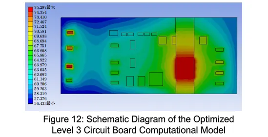
As noted earlier, high-power components are located on Layer 2 and Layer 4, which share identical parameters. Therefore, Layer 2 is selected for targeted analysis. The corresponding temperature calculation results are illustrated in Figures 6 through 8.

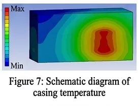
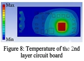
Table 4 Maximum junction temperature of components on each layer circuit board (°C)
| Layer Name | Maximum Junction Temperature |
| Chassis casing | 63.6 |
| 1st layer PCB | 70.9 |
| 2nd layer PCB | 143.6 |
| 3rd layer PCB | 74.7 |
| 4th layer PCB | 141.8 |
4.2 Optimization Methodology and Results
Considering the specific operational environment and safety requirements of spaceborne equipment, the thermal design principles must adhere to two core criteria:
Prioritize Passive Thermal Control: Minimize or entirely avoid reliance on active thermal control systems.
Maximize Reliability: Utilize mature, simple, and highly feasible technologies to ensure the overall reliability of the equipment.
As previously established, the heat dissipation channels for these components include thermal radiation and thermal conduction. Given the space environment context (which excludes forced convective heat transfer) and the relatively minor contribution of radiative heat exchange to the overall heat rejection process, this optimization design focuses strictly on thermal conduction.
The core objective of thermal optimization is to minimize the thermal resistance between the heat source and the cold sink. This is typically achieved by either altering material parameters or establishing new heat transfer pathways.
For the overheating high-power component in this study, the optimization strategy was determined through the following logical constraints:
Material Constraints: Adjusting material parameters is highly difficult due to manufacturing and performance compatibility limitations.
PCB Limits: The original design has already maximized the PCB’s thermal conduction capacity via internal copper cladding layers, leaving minimal room for further improvement along this specific path.
Consequently, the core direction of the thermal optimization design is to construct a new, dedicated heat dissipation pathway for the component, breaking through the existing thermal bottlenecks. Aerospace design must not only account for extreme environmental impacts on internal components but also elevate the cooling efficiency to meet strict high-reliability demands.
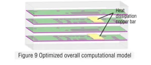
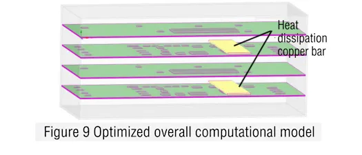
Based on these considerations, the adopted passive thermal optimization method involves installing a thermally conductive copper strip directly onto the casing surface of the overheating chip.
Material: Pure Copper
Thermal Conductivity: 396.7 W/(m·K) (Note: Unit corrected to standard engineering metric from original text)
Dimensions: 1 mm (Thickness) × 35 mm (Width) — precisely sized to cover the overheating component’s surface.
Connection Mechanism: The copper strip is welded directly to the equipment chassis housing and interfaced with the chip surface using a thermally conductive adhesive (TIM).
This establishes a direct thermal bridge, bypassing the traditional “Chip → PCB → Chassis” route. Because the thermal conductivity of pure copper is vastly superior to that of the PCB substrate, it significantly reduces the thermal resistance between the chip and the chassis. The ultimate goal is to rapidly conduct heat away from the silicon and lower the temperature of the overheating component.
For the remaining low-to-medium power components, their temperatures remain well within the expected junction temperature limits. Therefore, no dedicated cooling measures are implemented; they will continue to rely on the original design, transferring heat sequentially through the chip casing, PCB, and chassis.
The revised computational model, reflecting this thermal optimization methodology, is illustrated in Figure 9.
Holding all other parameters constant, the thermal simulation was re-executed to evaluate the updated temperature fields. The results of this optimized model are presented in Figures 10 through 12.
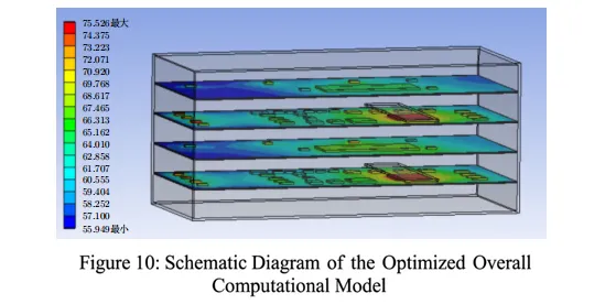
The optimized simulation results were subsequently compared against the physical experimental data. The maximum observed junction temperatures consistently appeared on Layer 2 and Layer 4, with specific measured values of 74.40°C and 74.57°C, respectively. The error margin between the simulation and the experimental results for these critical power devices was exceptionally low at < 1.25%.
Compared to the preliminary design, the discrepancy between the simulated and experimental values actually decreased. This improvement occurs because the overall temperature differential (maximum vs. minimum) across the board is now significantly smaller, thereby minimizing the thermal influence on the low-power components. Given that the location of the maximum error remains a non-critical factor in the overall analysis, the optimized simulation results retain a high degree of engineering validity.
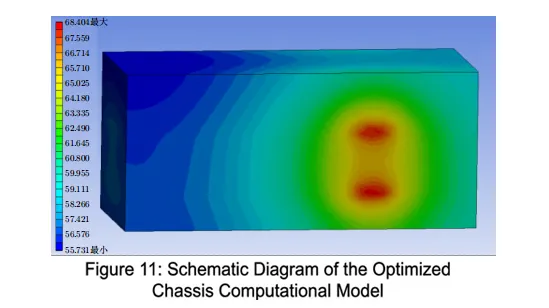
As illustrated in Figure 11, once the thermal load from the overheating component is conducted directly to the chassis housing via the thermally conductive copper strip, the overall temperature of the exterior casing increases compared to the baseline model. The highest temperatures on the casing are now distinctly concentrated at the physical connection point of the copper strip.
As detailed in Table 5, the thermal optimization yielded substantial, quantifiable improvements:
Layer 2 High-Power Component: Junction temperature plummeted from the original 143.6°C down to 75.3°C.
Layer 4 High-Power Component: Junction temperature plummeted from the original 141.8°C down to 75.5°C.
This represents a highly significant heat dissipation effect. The high-power components have successfully reached their expected normal operating junction temperatures (well below the < 80°C threshold), confirming that the optimization methodology fully satisfies the strict aerospace thermal design requirements.
Table 5 Maximum junction temperature of each layer before and after optimization (°C)
| Layer Name | Maximum junction temp before optimization | Maximum junction temp after optimization |
| Chassis casing | 63.6 | 68.4 |
| 1st layer PCB | 70.9 | 69.9 |
| 2nd layer PCB | 143.6 | 75.3 |
| 3rd layer PCB | 74.7 | 71.7 |
| 4th layer PCB | 141.8 | 75.5 |
5. Conclusion
This study established a heat transfer model for a specific spaceborne electronic device to simulate the PCB temperature distribution under a preliminary thermal design. Through this simulation, critical high-power components prone to overheating were identified, and the computational model’s high reference value was validated through physical experimentation.
Adhering to the core principles of thermal optimization for aerospace environments, a mature and highly feasible passive cooling strategy was implemented. By integrating thermally conductive copper strips onto the surfaces of overheating components, a dedicated secondary heat transfer pathway was established, effectively bypassing existing thermal resistance bottlenecks.
A secondary simulation of the optimized model demonstrates a significant reduction in junction temperatures, ensuring that all high-power components operate reliably even under the most extreme external thermal conditions. Furthermore, this optimization methodology strictly complies with established aerospace thermal design standards, offering exceptional feasibility and mission-critical reliability for satellite applications.
Struggling with Localized Overheating in Your PCB Design?
Standard cooling isn’t enough for high-TDP components in vacuum or high-altitude environments. If your simulation shows junction temperatures exceeding 80 °C, you need a specialized thermal path.
EcoThsuerm’s Aerospace-Grade Thermal Solutions Include:
Custom Copper & Aluminum Heat Spreaders (Pure Copper C11000)
Integrated Heat Pipe & Vapor Chamber Assemblies
Vacuum Brazing for Flux-Free, High-Reliability Chassis Joining
Advanced TIM (Thermal Interface Material) Application
Ready to optimize your thermal design?
Send us your STEP files or thermal requirements today, and our engineers will provide a complimentary thermal feasibility review within 24 hours.