IGBT Thermal Models, Thermal Design and Cooling Solutions
An IGBT thermal model describes how power loss becomes heat, how that heat travels through the module, and how quickly the semiconductor junction responds to a change in load. It is the link between the electrical loss calculation and the cooling system. When the model is constructed and validated correctly, engineers can estimate junction temperature, compare package and cooling concepts, define operating limits and identify where thermal resistance should be reduced.
The model must represent more than a single headline value. Heat passes through the semiconductor die, die-attach layer, metallized ceramic substrate, baseplate or cooling surface, thermal interface and heat sink or liquid cold plate. Each section has resistance to heat flow, while the solid materials also store thermal energy. Contact quality, heat spreading, coolant temperature and non-uniform die losses further influence the result. A useful model therefore combines physical understanding with test data rather than treating the IGBT module as an ideal point heat source.
Why an IGBT Thermal Model Is Necessary
The semiconductor junction is normally the most temperature-sensitive location in an IGBT module, yet it is enclosed within the package and cannot usually be measured directly during normal operation. A thermocouple attached to the baseplate or cold plate records a boundary temperature, not the instantaneous junction temperature. The difference can be substantial during rapid changes in power because the junction heats before the rest of the package reaches equilibrium.
A thermal model closes this measurement gap. Electrical conduction and switching losses are applied as the heat input, and the model predicts the temperature rise between the junction and a defined reference point. That reference may be the module case, heat sink, coolant or ambient air. The definition matters: a junction-to-case resistance cannot be combined indiscriminately with a cooling-component rating referenced to a different temperature or measurement location.
The model also helps distinguish a continuous thermal problem from a transient one. A module operating at nearly constant load may be assessed mainly through steady-state resistance. A traction inverter, pulsed power supply or servo drive can experience repeated acceleration, overload and regenerative events. In these applications, the duration and spacing of the pulses determine whether heat remains concentrated near the die or spreads into the baseplate and cooling system before the next event begins.
Building the Thermal Path from the Package Structure
A conventional baseplate IGBT module contains several materials arranged in layers. The semiconductor dies are attached to a metallized ceramic substrate, often by soldering or sintering. Copper metallization carries current and spreads heat laterally. The substrate provides electrical insulation while conducting heat toward the baseplate. A second joining layer may connect the substrate to the baseplate, which then contacts an air-cooled heat sink or liquid cold plate through a thermal interface material.
For a uniform layer with one-dimensional heat flow, thermal resistance can be approximated as Rth = d/(kA), where d is the layer thickness, k is thermal conductivity and A is the effective heat-flow area. The relationship explains why a thinner bond layer, a more conductive material and a larger effective area usually reduce resistance. Real IGBT structures are not purely one-dimensional, however. The die is smaller than the substrate and baseplate, so heat spreads as it moves downward. Voids, surface roughness, metallization patterns and neighboring dies can change the effective area and create local temperature gradients.
Thermal capacitance represents the energy stored as a material changes temperature. It can be approximated as Cth = mcp, where m is mass and cp is specific heat capacity. A thin semiconductor die has relatively little thermal mass and responds quickly, while a copper baseplate or cold plate stores more energy and responds more slowly. Resistance and capacitance together determine the shape of the transient temperature curve.
Contact resistance deserves separate treatment because it cannot be calculated reliably from bulk conductivity alone. The thermal performance of a solder joint, sintered layer or module-to-cold-plate interface depends on bond-line thickness, void distribution, surface condition and pressure. These factors can vary from one assembly to another, making experimental calibration particularly valuable at interfaces.
Steady-State and Transient Junction Temperature
Under stable operating conditions, a simplified junction-temperature estimate can be written as Tj = Tref + Ploss × Rth,j-ref. Tref is the temperature at the selected reference point, Ploss is the power dissipated by the relevant die or device, and Rth,j-ref is the thermal resistance from the junction to that reference. This equation is useful for an initial thermal budget, but it assumes that the system has reached equilibrium and that the chosen resistance properly represents the heat-sharing conditions inside the module.
Transient operation requires thermal impedance rather than only steady resistance. The transient thermal impedance Zth(t) describes how much of the final temperature rise has developed after a given heating time. A very short pulse may heat mainly the die and die-attach region. As the pulse continues, heat reaches the ceramic, baseplate, interface and cooling component. This time-dependent behavior is why a module can tolerate a short overload that would be unacceptable as a continuous loss.
Repeated pulses must be evaluated as a sequence, not as isolated events. If the off-time is too short for the structure to cool, the temperature response accumulates until it reaches a periodic steady condition. The average junction temperature influences electrical loss, while the temperature swing influences fatigue in interconnects and joining layers. Both values are important: a design may remain below the maximum junction temperature yet still experience damaging thermal cycles.
Foster and Cauer Thermal Networks
Foster and Cauer networks are two common ways to represent transient thermal behavior with resistance-capacitance elements. A Foster model is frequently obtained by fitting an exponential curve to measured or simulated transient thermal impedance. Its branches reproduce the temperature response efficiently, which makes the model convenient for system simulation and loss-profile calculations. The individual Foster elements do not normally correspond directly to identifiable physical layers in the package.
A Cauer network arranges thermal resistance and capacitance as a ladder through the heat-flow path. This form is more physically interpretable because successive sections can be associated approximately with the die, attach layers, substrate, baseplate and external cooling structure. It is useful when engineers want to connect models at a defined boundary or investigate how a change in one section affects the complete path.
Neither form is inherently more accurate without suitable parameters. A fitted Foster network can reproduce the source impedance curve very closely, while a poorly parameterized Cauer network can be misleading despite its physical appearance. Mathematical conversion between the two forms is possible, but the converted elements should not automatically be assigned to real package layers. Boundary conditions, multi-chip heat interaction and the validity range of the original data must remain clear.
For a multi-chip IGBT module, a single self-heating curve may also be insufficient. Heat generated by one IGBT or diode can raise the temperature of adjacent dies. A thermal-impedance matrix with self-heating and cross-coupling terms provides a better representation when die spacing is small or loss distribution is strongly unbalanced. Three-dimensional simulation can be used to derive these terms, followed by reduction into a compact model for control or system-level calculations.
Connecting Electrical Losses to the Thermal Model
The quality of a temperature prediction cannot exceed the quality of the loss input. IGBT conduction loss depends on current, duty cycle and temperature-dependent voltage drop. Switching loss depends on DC-link voltage, current, switching frequency, gate drive, commutation inductance and junction temperature. The freewheeling diode contributes conduction and recovery losses, and these losses may occur at different locations and times from the IGBT losses.
Using one constant loss value for every operating point can hide the condition that actually creates the highest junction temperature. A practical analysis starts with the intended mission profile or load cycle, calculates the IGBT and diode losses over time, and applies them to the appropriate thermal nodes. The calculation should be iterated when temperature materially changes electrical behavior. This electrothermal feedback is particularly relevant near operating limits.
Loss distribution within the module also matters. Two modules with the same total dissipation can have different peak junction temperatures if one concentrates more loss in a smaller die area. Cooling design should therefore use device-level or die-level heat maps whenever the data are available, rather than spreading total module loss uniformly across the entire baseplate.
Package Materials and Thermomechanical Design
Reducing thermal resistance is only one objective of package design. The materials must also survive repeated expansion and contraction. Silicon, copper, ceramic, solder, sintered metal and baseplate alloys have different coefficients of thermal expansion. As temperature changes, this mismatch creates mechanical stress in die-attach layers, substrate joints, bond wires and terminal connections. The largest temperature swing does not always occur in the same layer as the highest absolute temperature, so both thermal and mechanical models may be needed.
Ceramic substrates illustrate the trade-off. Alumina offers established processing and electrical insulation. Aluminium nitride provides higher thermal conductivity but brings different cost, processing and reliability considerations. Silicon nitride can offer attractive mechanical strength and fracture resistance for demanding cycling environments. The appropriate choice depends on voltage insulation, heat flux, substrate dimensions, joining process, expected temperature cycling and commercial constraints. Selecting a material by conductivity alone can move the reliability problem to another interface.
Copper metallization and baseplates improve heat spreading, but greater thickness also changes stiffness, thermal mass and stress. Aluminium or copper bond wires remain common in traditional packages, while planar interconnects and copper clips can alter both electrical and thermal paths. Sintered die attach can withstand higher temperatures than some conventional solder systems, but process control, surface finish and pressure requirements are critical. Each material decision should be evaluated as part of the complete package stack.
The Module-to-Cooler Interface
After heat reaches the case or baseplate, it must cross into the external cooling component. This case-to-sink path can become a significant part of the total resistance. Metal surfaces touch only at microscopic high points, leaving air-filled gaps elsewhere. Thermal grease, phase-change material or another suitable interface layer fills these gaps, but the material must form a thin and continuous bond line.
The effective interface resistance depends on more than the conductivity printed on a material datasheet. Surface flatness, roughness, mounting pressure, screw sequence, material viscosity, voiding and long-term pump-out all affect the assembled result. Excess material can increase resistance because most interface materials conduct heat less effectively than the adjoining metal. Insufficient material leaves air gaps. The application process and mounting method therefore require the same validation as the cold plate itself.
For a liquid-cooled system, coolant inlet temperature is a more useful boundary condition than room temperature. The analysis should also include coolant temperature rise along the channel, local heat-transfer coefficients, flow distribution and heat spreading through the cold-plate wall. A low average coolant temperature does not guarantee a low junction temperature if flow bypasses the highest-loss region or if the plate surface is distorted.
Direct Liquid Cooling for IGBT Modules
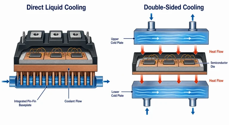
Direct liquid cooling shortens the external thermal path by integrating the module baseplate more closely with the coolant passage. Pin fins or other enhanced surfaces can be formed on the underside of the baseplate so that coolant removes heat without a separate conventional heat sink interface. Eliminating an interface and reducing conduction distance can lower the junction-to-fluid temperature difference and improve heat-flux capability.
The benefit depends on the entire hydraulic design. Pin-fin density, fin height, coolant velocity and flow direction influence heat transfer as well as pressure drop. Uniform flow is necessary to avoid a well-cooled inlet region and a hot downstream region. The cooler must also meet requirements for corrosion resistance, coolant compatibility, cleanliness, sealing and burst pressure. A thermally aggressive geometry that is difficult to manufacture or prone to blockage may not be the best production solution.
Direct cooling also changes how the power module and cold plate are manufactured and serviced. Brazed or welded joints, seals and coolant manifolds become part of the reliability path. Leak testing and contamination control are essential because failure can affect both the thermal system and high-voltage electronics. These considerations should be included at the concept stage rather than added after the thermal geometry has been frozen.
Double-Sided Cooling
Double-sided cooling creates two parallel heat-flow paths from the semiconductor region. Heat can leave through both the upper and lower sides of a planar package, reducing dependence on a single substrate and baseplate path. The concept is especially attractive where high power density, compact packaging and low parasitic inductance are required.
Achieving the theoretical advantage requires balanced mechanical and thermal design. The upper and lower cooling surfaces must maintain controlled contact without placing damaging stress on the semiconductor or interconnect layers. Electrical isolation, creepage distance, flatness and tolerance accumulation become more demanding when cooling structures approach both sides of the device. If one interface has much higher resistance than the other, the heat split will be uneven and the second path will contribute less than expected.
Double-sided structures can also complicate temperature measurement and assembly. A compact model should represent both branches and their coupling rather than simply dividing a single thermal resistance by two. Three-dimensional simulation is useful for checking current paths, local heat spreading and pressure distribution before reducing the result to a system model.
Double-Sided Cooling
Double-sided cooling creates two parallel heat-flow paths from the semiconductor region. Heat can leave through both the upper and lower sides of a planar package, reducing dependence on a single substrate and baseplate path. The concept is especially attractive where high power density, compact packaging and low parasitic inductance are required.
Achieving the theoretical advantage requires balanced mechanical and thermal design. The upper and lower cooling surfaces must maintain controlled contact without placing damaging stress on the semiconductor or interconnect layers. Electrical isolation, creepage distance, flatness and tolerance accumulation become more demanding when cooling structures approach both sides of the device. If one interface has much higher resistance than the other, the heat split will be uneven and the second path will contribute less than expected.
Double-sided structures can also complicate temperature measurement and assembly. A compact model should represent both branches and their coupling rather than simply dividing a single thermal resistance by two. Three-dimensional simulation is useful for checking current paths, local heat spreading and pressure distribution before reducing the result to a system model.
Phase-Change Structures and Press-Pack Devices
Heat pipes, vapor chambers and other phase-change structures can spread concentrated heat by evaporating and condensing a working fluid inside a sealed enclosure. In an IGBT cooling system, their principal value is often heat spreading or heat transport rather than replacing the final heat sink. They can connect a restricted module area to a larger fin stack or remote liquid-cooled surface. Orientation, operating temperature range, capillary limit and thermal contact on both sides must be considered before the technology is selected.
Press-pack IGBT devices use mechanical pressure to maintain electrical and thermal contact through a stack of internal elements. Their structure can support cooling from both sides and can be useful in high-current systems that value a pressure-contact architecture. Thermal performance depends strongly on contact pressure, surface condition, clamping uniformity and cooler flatness. A low nominal material resistance does not compensate for an uneven force distribution across the device.
The clamping system is therefore part of the thermal design. Pressure that is too low raises contact resistance, while excessive or non-uniform pressure can damage internal elements. The cooler, insulating parts and mechanical frame should be analysed together so that contact remains controlled across manufacturing tolerances and thermal expansion.
Choosing the Right Cooling Architecture
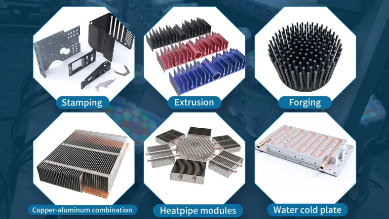
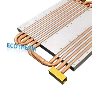
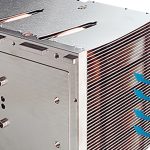
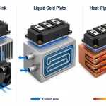
There is no universally best IGBT cooling method. Air cooling remains practical when heat loss is moderate, ambient temperature is controlled and sufficient fin volume and airflow are available. Conventional liquid cold plates provide higher heat-removal capability and tighter temperature control without requiring a fully integrated module structure. Direct liquid cooling becomes attractive when interface resistance and heat-flux density justify the additional sealing and manufacturing complexity. Double-sided cooling can provide the shortest parallel paths, but it demands a package and assembly designed around that architecture from the beginning.
The decision should be based on maximum and transient loss, coolant or ambient conditions, available volume, allowable pressure drop, electrical isolation, vibration, service life, leak-risk tolerance, production quantity and cost. The correct comparison is not only thermal resistance at a laboratory condition. It is the complete system’s ability to keep every die within its temperature limit throughout the intended mission profile while remaining manufacturable and reliable.
Early collaboration between electrical, mechanical, thermal and manufacturing teams usually produces a better result than sizing the cooler after the power stage is complete. Module position, busbar geometry, capacitor placement, channel routing and mounting stiffness interact. A small change to the mechanical layout can sometimes reduce spreading resistance or improve flow distribution more effectively than selecting a more expensive thermal material.
Validating the Thermal Model and Hardware
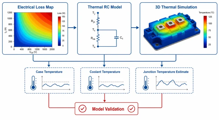
A credible model should be checked against physical measurements under controlled boundary conditions. The process begins with an electrical loss estimate that is consistent with the actual gate drive, switching condition and device temperature. The thermal model then predicts junction, case, cold-plate and coolant temperatures. Measured temperatures are compared with these predictions, and uncertain parameters such as contact resistance or convection coefficients are adjusted only within physically reasonable limits.
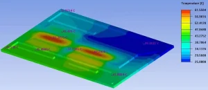
Thermocouples can measure selected case, baseplate, heat-sink and coolant locations. Infrared imaging can reveal surface temperature patterns when emissivity and optical access are controlled. Coolant inlet and outlet measurements support an energy balance, although small temperature differences require accurate sensors and stable flow. Junction temperature may be estimated using a calibrated temperature-sensitive electrical parameter or another validated indirect method when direct sensing is not possible.
Steady-state testing confirms the overall resistance and energy balance, while transient testing checks the RC time constants. A model fitted only to one steady operating point may still predict a fast overload incorrectly. Conversely, a junction-to-case transient curve alone does not validate the external cold plate, interface or coolant network. Both the internal and external portions must be tested at their defined boundaries.
Validating the Thermal Model and Hardware
A credible model should be checked against physical measurements under controlled boundary conditions. The process begins with an electrical loss estimate that is consistent with the actual gate drive, switching condition and device temperature. The thermal model then predicts junction, case, cold-plate and coolant temperatures. Measured temperatures are compared with these predictions, and uncertain parameters such as contact resistance or convection coefficients are adjusted only within physically reasonable limits.
Thermocouples can measure selected case, baseplate, heat-sink and coolant locations. Infrared imaging can reveal surface temperature patterns when emissivity and optical access are controlled. Coolant inlet and outlet measurements support an energy balance, although small temperature differences require accurate sensors and stable flow. Junction temperature may be estimated using a calibrated temperature-sensitive electrical parameter or another validated indirect method when direct sensing is not possible.
Steady-state testing confirms the overall resistance and energy balance, while transient testing checks the RC time constants. A model fitted only to one steady operating point may still predict a fast overload incorrectly. Conversely, a junction-to-case transient curve alone does not validate the external cold plate, interface or coolant network. Both the internal and external portions must be tested at their defined boundaries.
Caption: A reliable thermal model is calibrated and validated against measured boundary temperatures and an estimated junction-temperature response.
Validation should cover more than a new assembly. Thermal cycling, power cycling, vibration and coolant aging can change interfaces, seals and contact pressure. Repeating key thermal measurements after reliability testing reveals whether the heat path has degraded. For production, flatness, mounting torque, interface-material application, coolant flow and leak-test criteria should be controlled so that the validated prototype performance can be reproduced.
Common Thermal-Modelling Errors
One common error is using the module’s maximum junction temperature as the normal design target. That value is an absolute limit, not a recommended continuous operating point. Measurement uncertainty, loss variation, coolant-temperature tolerance, manufacturing variation and aging all require margin.
Another error is adding thermal-resistance values that do not share compatible reference planes or test conditions. Junction-to-case data measured with an isothermal case cannot represent a real baseplate with non-uniform cooling unless the difference is addressed. Likewise, a cold-plate resistance referenced to average surface temperature may not combine directly with a module model referenced to a local point.
Applying total module loss to a single node can also underpredict the hottest die. The IGBT and diode may have different loss profiles, and neighboring chips exchange heat. Finally, tuning uncertain parameters until simulation matches one measurement can create a model that is accurate only at that operating point. Validation across multiple power levels, flow rates and transient durations is a stronger test of whether the model represents the physics.
Frequently Asked Questions
What is the difference between a Foster and a Cauer thermal model?
A Foster model is commonly used to fit transient thermal-impedance data with a compact set of exponential terms. A Cauer model uses a ladder structure that more naturally represents successive sections of the physical heat path. Foster models are convenient for reproducing a measured response, while Cauer models are often easier to connect to package layers and external cooling components. The correct choice depends on the simulation purpose and the quality of the parameters.
How is IGBT junction temperature calculated?
For a stable load, junction temperature can be estimated from the reference temperature plus power loss multiplied by the corresponding thermal resistance. For changing loads, the time-dependent loss profile must be convolved with the transient thermal impedance or applied to an equivalent RC network. Accurate loss data, compatible boundary definitions and validation measurements are essential.
Why is transient thermal impedance important for an IGBT?
Transient thermal impedance shows how quickly temperature rises after power is applied. It allows engineers to evaluate short overloads, pulsed operation and repeated load cycles that cannot be described by a steady thermal-resistance value alone. It also helps estimate junction-temperature swing, which is closely related to package fatigue.
Does direct liquid cooling always outperform a conventional cold plate?
Direct liquid cooling can remove interfaces and shorten the heat path, but the result depends on flow distribution, pressure drop, baseplate geometry, coolant conditions and manufacturing quality. A well-designed conventional cold plate may be preferable when serviceability, sealing simplicity or module standardization is more important than the lowest possible thermal resistance.
When should double-sided IGBT cooling be considered?
Double-sided cooling is worth considering when power density and package volume justify two parallel heat paths and when the electrical and mechanical architecture can support cooling on both sides. It should be planned at package level because insulation, flatness, pressure, interconnects and assembly tolerance all affect performance.
What information is needed to develop an IGBT cooling solution?
The essential inputs are the module or die layout, IGBT and diode loss profiles, maximum allowable junction temperature, transient duty cycle, ambient or coolant temperature, installation envelope, electrical-isolation requirements and reliability targets. A liquid-cooled design also needs coolant type, flow-rate range, allowable pressure drop, corrosion requirements and connection details.
Discuss an IGBT Thermal-Management Project with Ecothermgroup
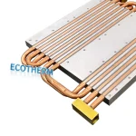
Ecothermgroup develops custom heat sinks and liquid cold plates for power electronics, including inverter and IGBT applications. A useful project review begins with the module drawing, heat-loss map, duty cycle, cooling boundary conditions, mounting method and available space. These inputs allow the internal thermal model, module interface and external cooler to be considered as one continuous heat path. Visit the Ecothermgroup website to discuss a cooling solution for your application.